+86-13760153421
sales@pcbahub.com
High-Quality PCB Manufacturer - Custom HDI & Multi-layer PCB
  • Home
  • PCB FAB
    HDI PCB Board High Layer PCB High Frequency PCB High Speed PCB 5G Optical Module PCB Semiconductor PCB Thick Copper PCB Industrial Control PCB Consumer Electronics PCB Flex/Rigid-Flex PCB RF Antenna PCB Alu/Led PCB
  • PCB Assembly
    Medical electronics Communication electronics Automotive electronics Consumer electronics Smart home Industrial control OEM/EMS PCBA product
  • Capabilities
    PCB capabilities PCBA capabilities Components SMD stencil Files requested for pcb/pcba
  • About Us
    About pcba hub VR factory visit Certificate FAQ(frequently asked questions)
  • News
    Blogs R&D Updates
  • Contact
  • Language
  • En
    English 中文版
  • PCB/PCBA QUOTE

PCB/PCBA Online Quote

PCS
Gerber & BOM Files

1. Please upload the Gerber & BOM Files and board making instructions

2. The uploaded file format supports ZIP, RAR, 7Z compression package, less than 50MB

1. Please upload the Gerber Files and board making instructions

2. The uploaded file format supports ZIP, RAR, 7Z compression package, less than 50MB

1. Please upload the BOM Files

2. The uploaded file format supports ZIP, RAR, 7Z compression package, less than 50MB

RF Antenna PCB

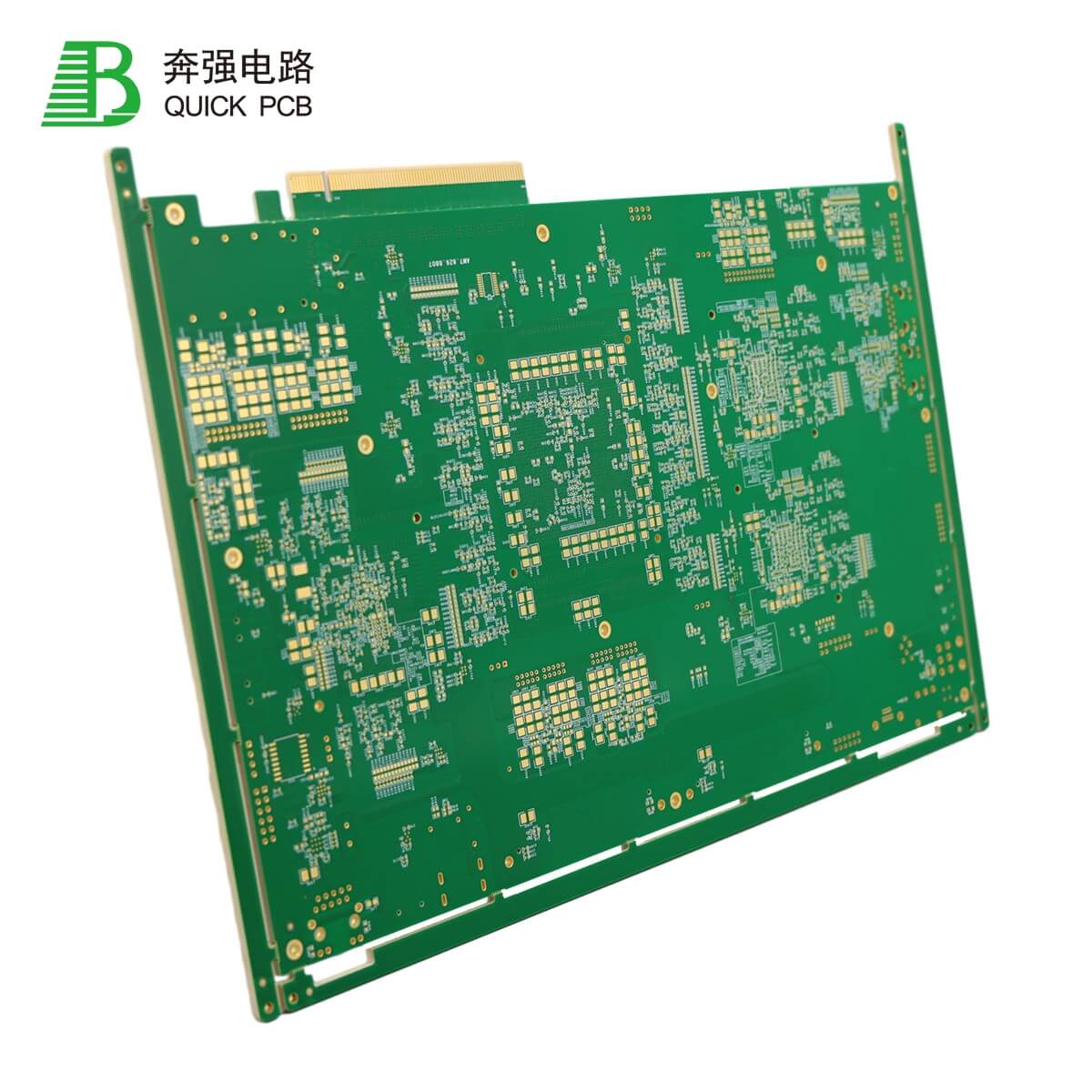
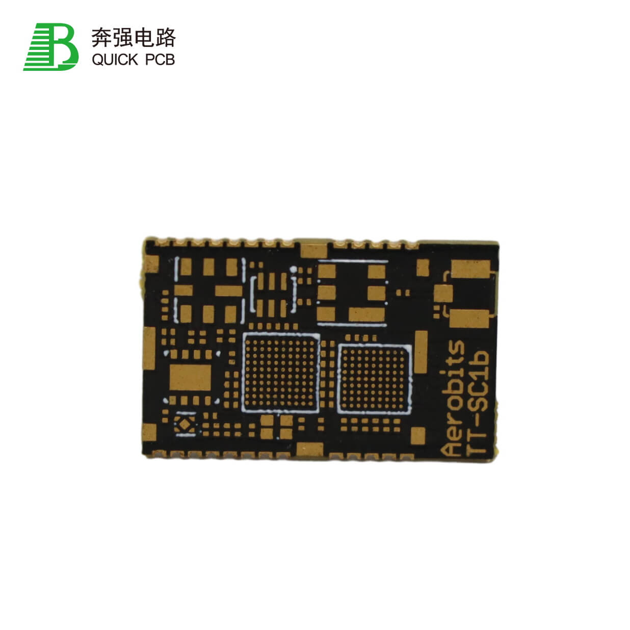
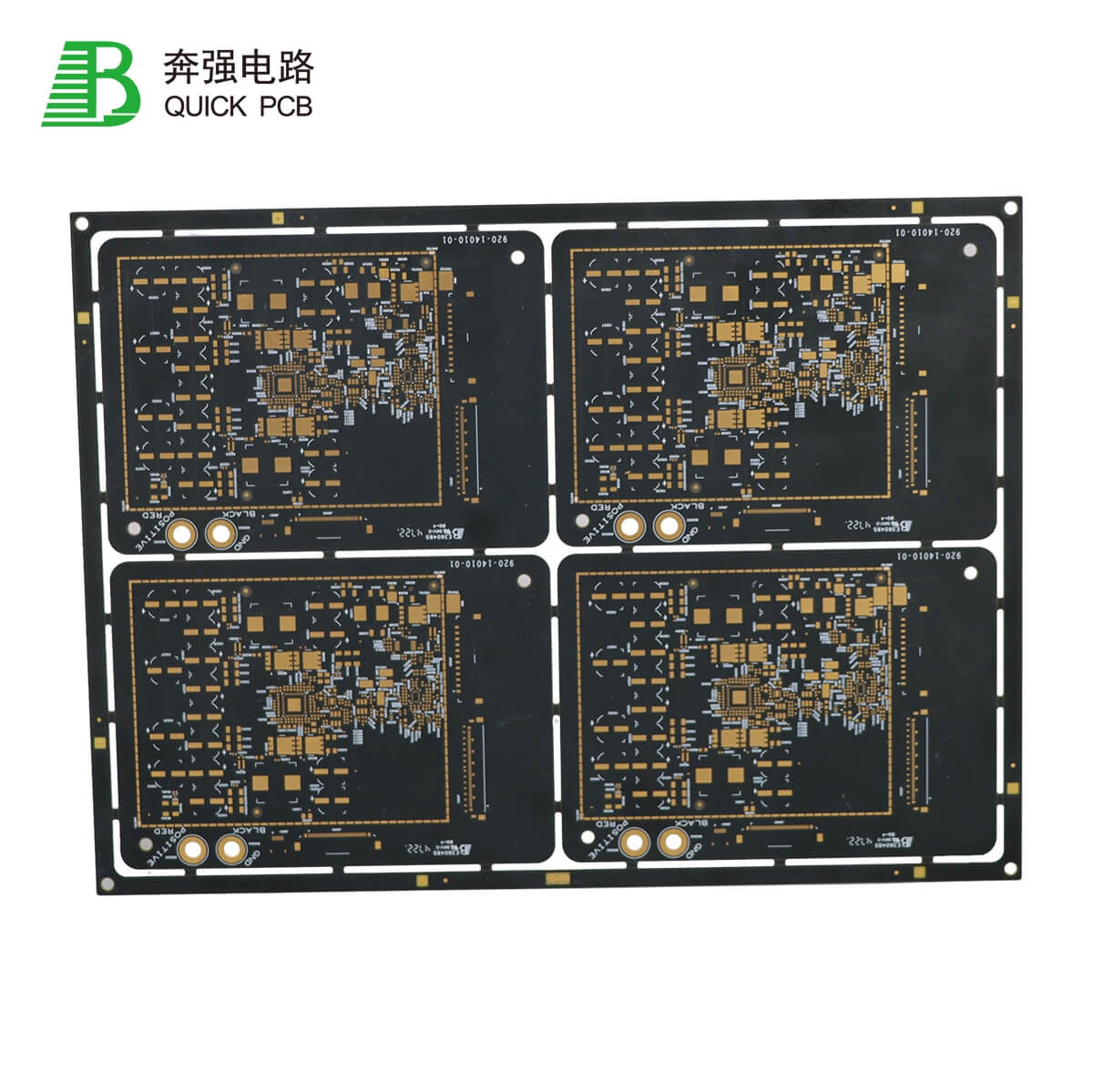
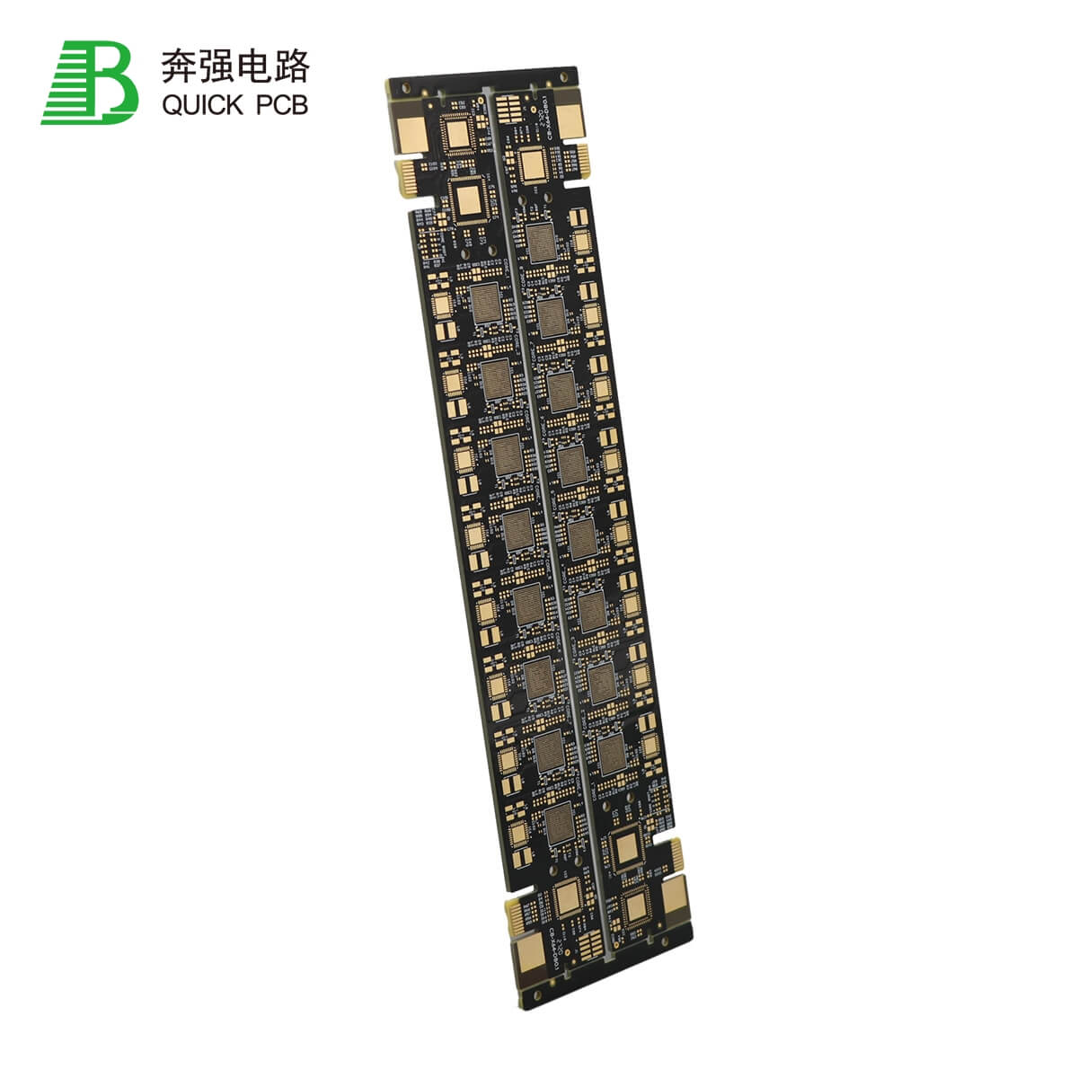
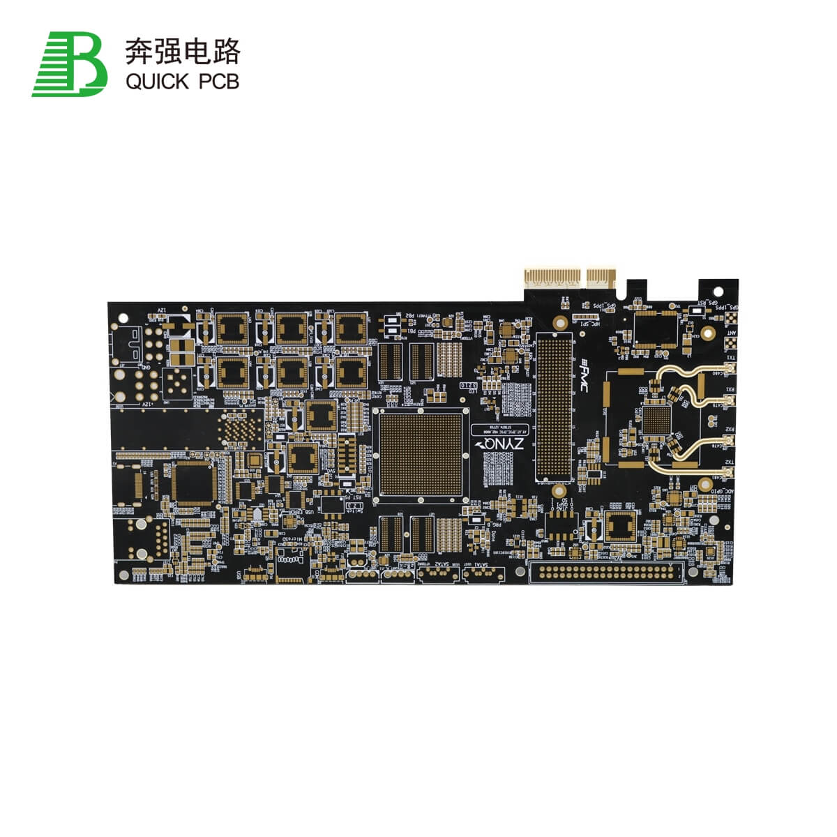
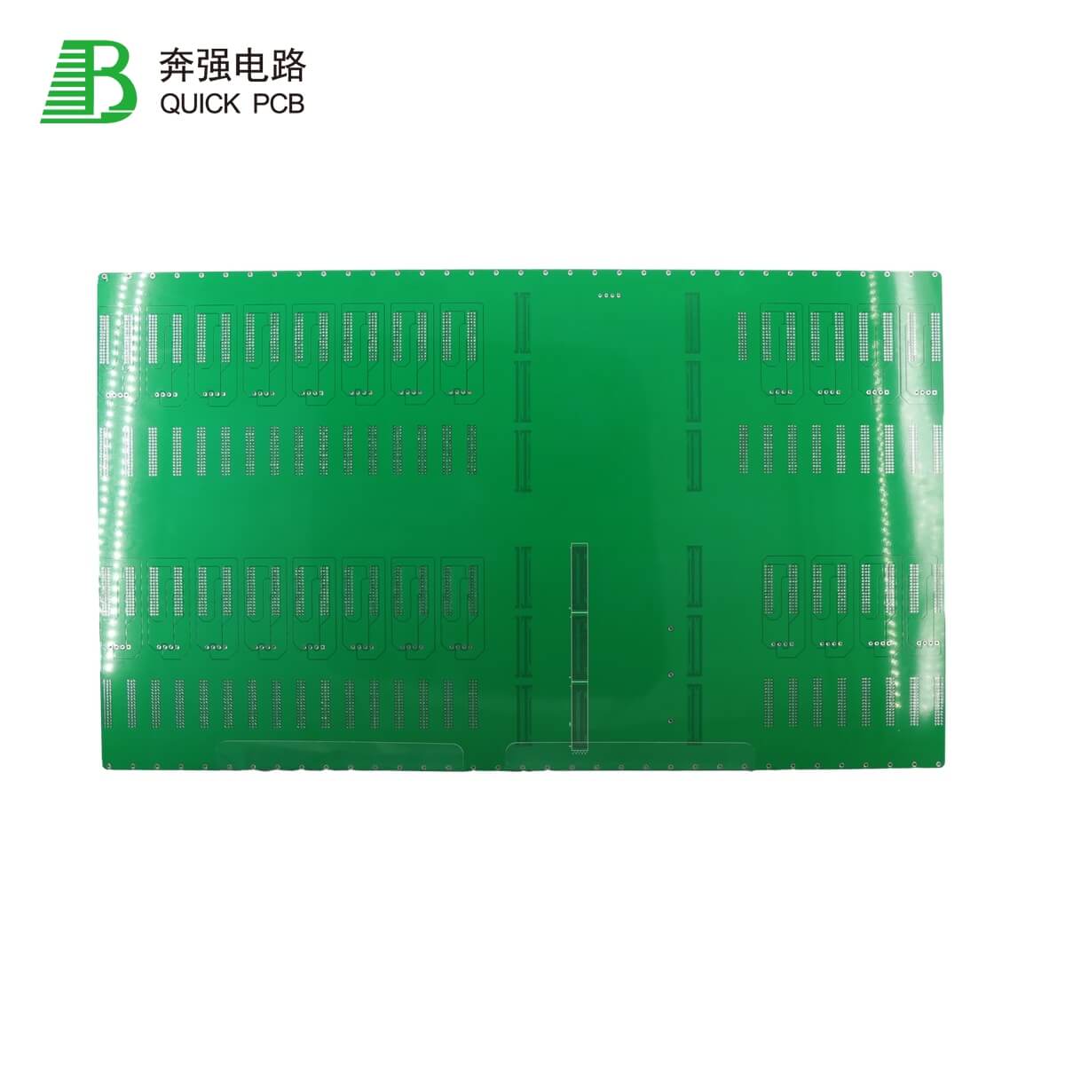
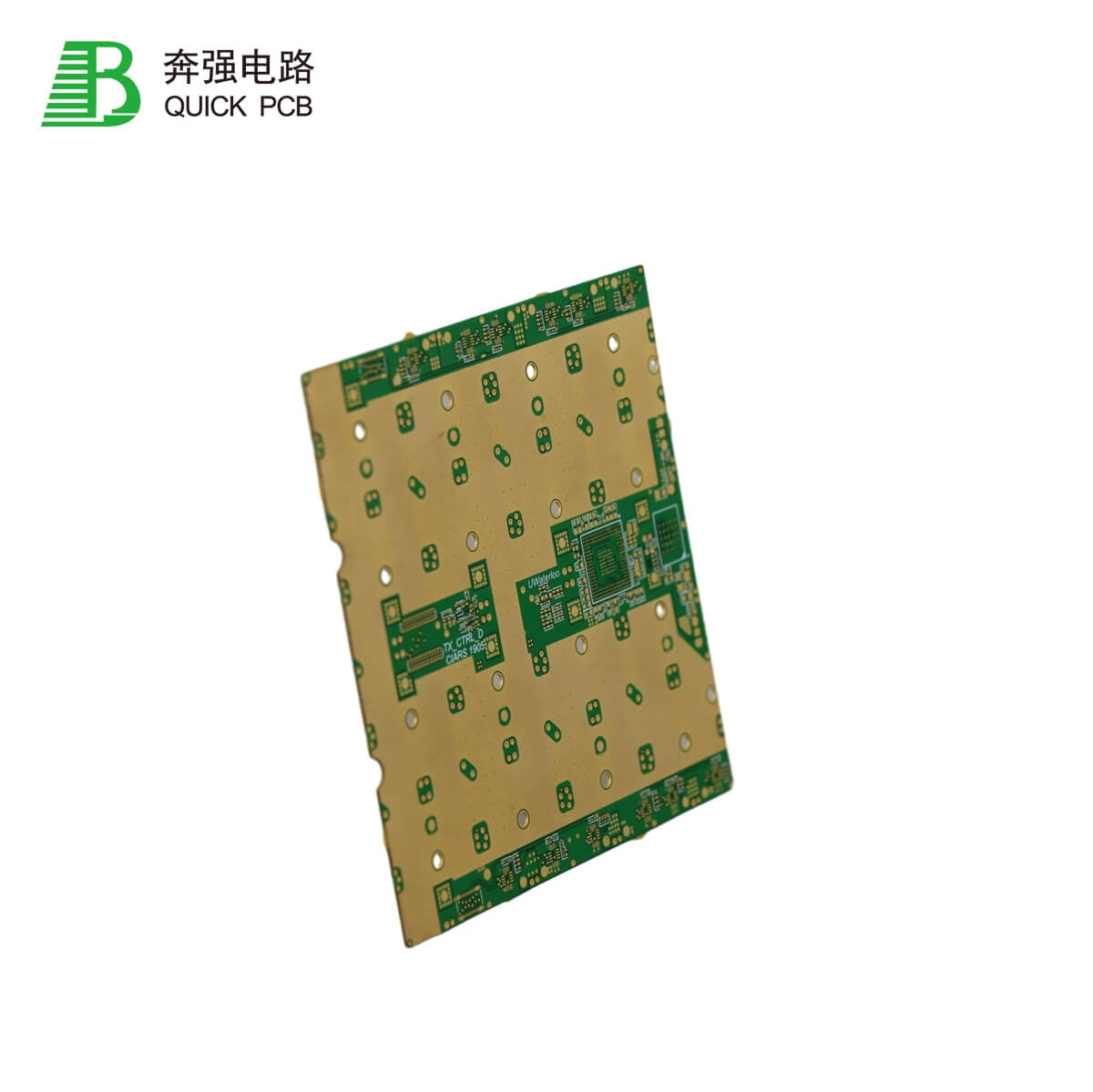
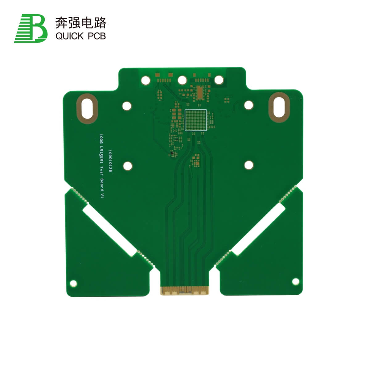
Discover our RF antenna PCB solutions, optimized for high-frequency performance in RF applications, ensuring reliable signal transmission and quality.

RF Antenna PCB
  • Home
  • PCB FAB
  • RF Antenna PCB

Product center

  • HDI PCB Board
  • High Layer PCB
  • High Frequency PCB
  • High Speed PCB
  • 5G Optical Module PCB
  • Semiconductor PCB
  • Thick Copper PCB
  • Industrial Control PCB
  • Consumer Electronics PCB
  • Flex/Rigid-Flex PCB
  • RF Antenna PCB
  • Alu/Led PCB
  • PCBA product
RF Antenna PCB 44

RF Antenna PCB 44

Semiconductor Field Test Probe Card 36 layers 2+N+2 Board Thickness: 4.8 mm Minimum Hole Size: 0.2 mm Hole-to-Line Distance: 0.14 mm

Product Details

RF Antenna PCB 43

RF Antenna PCB 43

Semiconductor Field Test 16 layers 7-step HDI 7+N+7 HDI Thickness: 2.4 mm Minimum hole size: 0.15 mm Hole-to-line distance: 0.07 mm Minimum line width/distance: 0.055/0.055 mm Surface Finish: ENIG

Product Details

RF Antenna PCB 42

RF Antenna PCB 42

Application Characteristic Material Layer Communication High speed+high TG material IT968TC+Shengyi S1000-2M 10L Thickness Min hole diameter Min width/space Internal Number 1.00.1mm Laser hole: 0.10mm, Mechanical hole 0.15mm 100/100um S221021G10 Surface f

Product Details

RF Antenna PCB 41

RF Antenna PCB 41

Application Characteristic Material Layer Communication High speed+high TG material IT968TC+Shengyi S1000-2M 10L Thickness Min hole diameter Min width/space Internal Number 1.00.1mm Laser hole: 0.10mm, Mechanical hole 0.15mm 100/100um S221021G10 Surface f

Product Details

RF Antenna PCB 40

RF Antenna PCB 40

Step golden finger board Material: TU-872SLK 22 layers 1-step HDI 1+N+1 HDI Thickness: 3.0 mm Minimum hole size: 0.25 mm Hole-to-line distance: 0.13 mm Surface Finish: ENIG + Gold finger + Back drill

Product Details

RF Antenna PCB 39

RF Antenna PCB 39

Application Characteristic Material Layer Communication High speed+high TG material IT968TC+Shengyi S1000-2M 10L Thickness Min hole diameter Min width/space Internal Number 1.00.1mm Laser hole: 0.10mm, Mechanical hole 0.15mm 100/100um S221021G10 Surface f

Product Details

RF Antenna PCB 38

RF Antenna PCB 38

Application Characteristic Material Layer Communication High speed+high TG material IT968TC+Shengyi S1000-2M 10L Thickness Min hole diameter Min width/space Internal Number 1.00.1mm Laser hole: 0.10mm, Mechanical hole 0.15mm 100/100um S221021G10 Surface f

Product Details

RF Antenna PCB 37

RF Antenna PCB 37

Application: Computer Product Features: 2x Laser drilling, 3x Pressfit, 2-step HDI board Material: Shengyi S1000-2M Layers: 10L Board Thickness: 1.60.16mm Minimum Hole Size: Laser hole: 0.127mm; Mechanical hole: 0.20mm, Aspect ratio: 8:1 Minimum Line Widt

Product Details

RF Antenna PCB 36

RF Antenna PCB 36

Semiconductor Field Interposer 14 layers 4-step HDI 4+N+4 HDI Thickness: 2.6 mm Minimum hole size: 0.1 mm Hole-to-line distance: 0.1 mm Minimum line width/spacing: 0.06/0.09 mm

Product Details

RF Antenna PCB 35

RF Antenna PCB 35

Fixture Test Board 4 layers Surface Finish: ENIG Minimum Line Width/Spacing: 0.05/0.05 mm Impedance Tolerance: +/-8%

Product Details

RF Antenna PCB 34

RF Antenna PCB 34

Application Characteristic Material Layer Communication High speed+high TG material IT968TC+Shengyi S1000-2M 10L Thickness Min hole diameter Min width/space Internal Number 1.00.1mm Laser hole: 0.10mm, Mechanical hole 0.15mm 100/100um S221021G10 Surface f

Product Details

RF Antenna PCB 33

RF Antenna PCB 33

Application Characteristic Material Layer Communication High speed+high TG material IT968TC+Shengyi S1000-2M 10L Thickness Min hole diameter Min width/space Internal Number 1.00.1mm Laser hole: 0.10mm, Mechanical hole 0.15mm 100/100um S221021G10 Surface f

Product Details

RF Antenna PCB 32

RF Antenna PCB 32

High Speed Chip Server Card Material: TU-872SLK + RO4350 16 layers Board Thickness: 1.6 mm Minimum Line Width/Spacing: 0.075/0.075 mm Surface Finish: ENIG + Gold finger

Product Details

RF Antenna PCB 31

RF Antenna PCB 31

Application Characteristic Material Layer Communication High speed+high TG material IT968TC+Shengyi S1000-2M 10L Thickness Min hole diameter Min width/space Internal Number 1.00.1mm Laser hole: 0.10mm, Mechanical hole 0.15mm 100/100um S221021G10 Surface f

Product Details

RF Antenna PCB 30

RF Antenna PCB 30

Application Characteristic Material Layer Communication High speed+high TG material IT968TC+Shengyi S1000-2M 10L Thickness Min hole diameter Min width/space Internal Number 1.00.1mm Laser hole: 0.10mm, Mechanical hole 0.15mm 100/100um S221021G10 Surface f

Product Details

RF Antenna PCB 29

RF Antenna PCB 29

100G Optical Communication Module Material: R-5775G 10 layers 2-step HDI 2+N+2 HDI Surface Finish: Nickel plated palladium

Product Details

  • Previous
  • 1
  • 2
  • 3
  • 4
  • Next
  • 4 Page60 Records
High-Quality PCB Manufacturer - Custom HDI & Multi-layer PCB

Service Hotline

+86-13760153421
Email: sales@pcbahub.com

address

Building C5/B6, Yanchuan North Industrial Park, Yanluo Street, Baoan , Shenzhen, China

ORDER ONLINE

PCB/PCBA

HDI PCB Board
High Layer PCB
High Frequency PCB
High Speed PCB
Industrial control
Communication electronics
OEM/EMS

About Us

About pcba hub
VR factory visit
Certificate
FAQ(frequently asked questions)

Quick links

News
Contact
Language
Copyright © 2005-2024 BenQiang Circuit Co. Ltd. All Rights Reserved.
map
  • Message
  • E-mail

    sales@pcbahub.com

  • Linkedin

    https://linkedin.com/company/quickpcb

  • WhatsApp

    +86 13760153421